View
Schematic View
Read a load board the way you review one: the DUT on the first sheet, every series termination in signal order, both legs of each Kelvin connection, and the tester channel on each net taken from your saved channel plan. Then change it in place: add a part, change a value, rename a net. Every edit is checked before it lands, and any of the last 50 states can be restored.
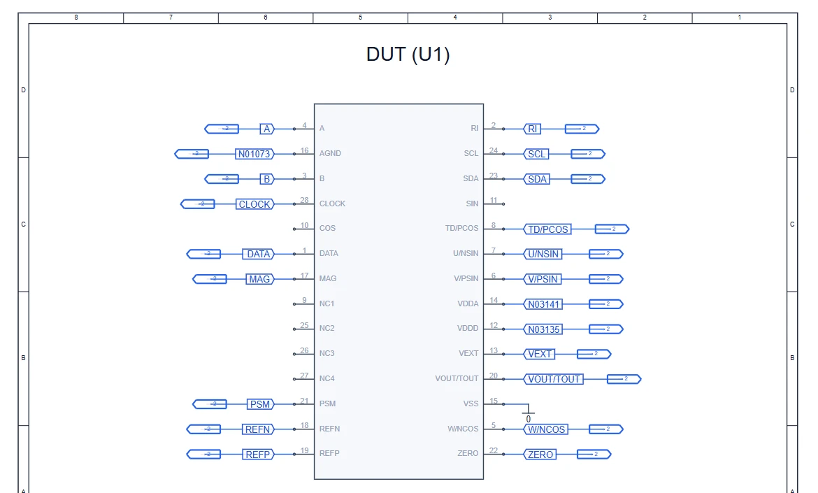
Sheets in the order you review a DIB
A load-board schematic has a natural reading order: what is the DUT, what sits between it and the tester, and which tester resource each pin lands on. The engine paginates the board in that order instead of packing everything onto one canvas.
1 · The DUT
Drawn once, on the first sheet. Every pin leaves through an off-page connector to the sheet its net continues on.
2 · The circuitry between
One sheet per functional block, such as power and decoupling, or signal conditioning with its terminations and ESD parts.
3 · The tester resources
One sheet per instrument slot, its channels listed down a column in channel order, each wired to the DUT net it lands on.
A net that crosses sheets carries a connector at both ends, so you can follow any pin from the tester to the DUT and back. A board with no channel plan is drawn as a plain schematic: the DUT sheet, then one sheet of supporting parts.
Drawn with the conventions a DIB needs
A general-purpose schematic tool draws a load board like any other circuit. The ATE schematic engine draws it the way test engineers read one.
Terminations in signal order
Tester channel, then series resistor, then DUT pin. The channel flag sits on the tester side of the resistor, so the drawing never shows a channel bypassing its termination.
Both Kelvin legs
Force and sense are drawn as separate nets to the instrument, never collapsed into a single wire.
Decoupling as banks
Capacitors that share a supply and ground are drawn as one parallel bank on a single supply trunk and a single ground trunk, not scattered across the sheet.
Drawn shorts checked, label pile-ups cleared
Each sheet is checked for a wire of one net touching another net's wire. Overlapping net labels are moved apart, and a move is kept only when a fresh render shows fewer overlaps.
Drag a part to where you want it and the move is stored with the design: it survives every re-render, and the wires follow it.
Tester channels from the saved plan
Channel flags, the tester-channel annotations on each net, come from the project's saved channel plan, not from a label someone typed on a drawing. The flags, the generated program's channel map and the DIB check all read that one saved plan. A channel you saved is drawn as decided. A channel the auto-assigner only proposed from the tester configuration is drawn marked "(proposed)", so a suggestion is never mistaken for a decision.
Edit in place, restore any state
Change the design where you are reading it. Ask for an edit in plain words from the edit chat docked on the design page, for example a pull-up on a named net, and the IG-XL agent applies it to that board. The same edits are available through the REST API.
| Edit | What it changes |
|---|---|
| Add a passive | A resistor or capacitor with the value you give, between two existing nets. |
| Add a library part | A part from the reference library, arriving with its real pins wired to the nets you name. A part the library does not hold is refused, never invented. |
| Change a value | The value of an existing resistor or capacitor. |
| Rename a net | The net's name, on every sheet that carries it. |
| Connect or disconnect a pin | One pin joined to an existing net, or taken off it. |
| Remove a component | The part, its symbol and footprint, and any trace that served only its pins. |
| Rotate a component | On the schematic, in steps of 90°. |
Every edit is checked before it is saved: an edit that would leave the board with more errors than it had is refused and never reaches your design. When one lands, every sheet re-renders from the stored design and the board's checks run again. Undo reverts the last edit. The History dropdown in the design header lists the newest 50 states (each edit, undo and restore) and restores any one of them. A restore is recorded too, so going back never loses what came after.
Where schematics come from
| Source | What you get |
|---|---|
| Allegro netlist or Fabmaster export | The netlist triad (pstchip, pstxnet, pstxprt) and Fabmaster exports import natively, with no Cadence licence, into a design with a synthesized schematic: labelled parts on a grid, with the DUT on a sheet of its own first when the engine recognises one. |
| KiCad | .kicad_sch files are picked up automatically from synced repositories, with the layout when a matching .kicad_pcb sits beside them. |
| PDF drawing | Multi-page schematic PDFs import into a design with a netlist, one sheet per page, shown as drawn. Useful for boards where the drawing is all you have. |
| Layout exports | IPC-2581, ODB++ and DSN layouts bring in copper and nets, with no schematic of their own. See PCB Layout. |
| Your own edits | Any of the above, changed in place (§04). |
For a design review, the print view renders every sheet one per page for the browser's Save as PDF. The board at the top of this page is a real, CC0-licensed Allegro 17 export with 12 components, 23 nets and 68 pins. Its pin match and board checks are on Board Intelligence.
One design, schematic and copper
The schematic, this page, is the logical board: components, nets and values. The layout is the physical copper: pads, traces, pours and drills. It comes from your CAD flow and is imported as drawn, then checked and exported on PCB Layout.
A design can hold a schematic alone, a schematic with its copper, or copper alone, stored in an open, MIT-licensed format. When the layout arrives as a separate import, it is bound to the schematic design it implements, and the binding is rechecked against both every time it is read. Every view reads the same design, and every design records which importer brought it in.