Layout
PCB Layout
Bring in the routed board as your CAD tool wrote it, then work with the copper: zoom through it in 2D, turn it over in 3D, measure it against fab rules, light up the traces behind a requirement, and export the Gerbers, fab package, BOM and pick-and-place the board house needs. The copper stays exactly as your CAD tool laid it out; ATE·IQ reads and measures it, and never routes it.
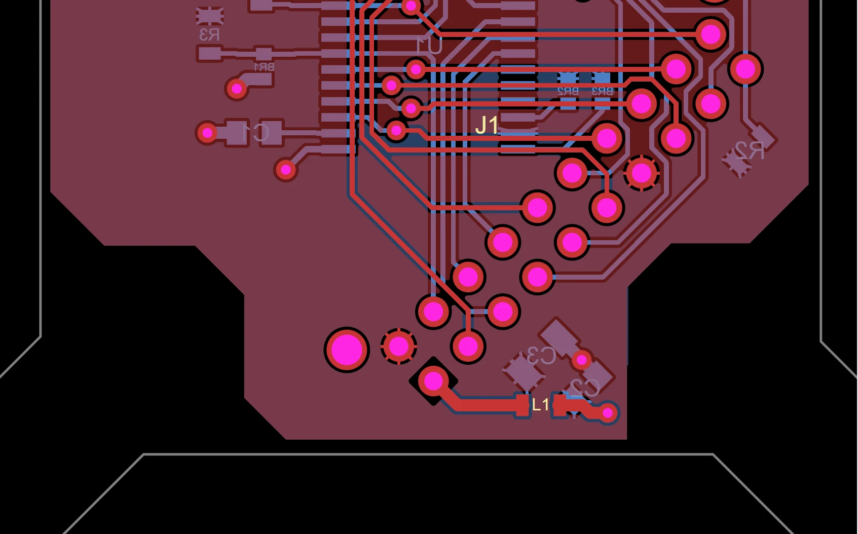
Import the board as it was routed
A load board usually already exists somewhere: at a PCB vendor, in a legacy archive, or in the layout engineer's CAD tool. Pick the export from the Import menu, or let a synced repository bring it in, and the copper lands as drawn, with the importer that brought it recorded on the design.
| Format | Extension | What comes in |
|---|---|---|
| Allegro Fabmaster | .txt / .fab | Pads, plated holes, vias, every etch line and arc, the outline, and copper pours drawn as cut with their voids. A native parser, no Cadence licence. See EDA Import & Export. |
| IPC-2581 | .xml / .cvg | Components, nets, layers and copper. Allegro's IPC-2581 exporter folds every artwork film it cannot map by name into the last copper layer; ATE·IQ rebuilds the real copper layer from the padstacks and component sides, and the import notes list what it set aside. |
| ODB++ | .tgz | The layer matrix, EDA data and per-layer features, with real copper. |
| Specctra DSN | .dsn | KiCad, Allegro and EAGLE dialects. Pads, traces, vias and drills; copper pours are not imported. |
| KiCad | .kicad_pcb | Picked up automatically from synced repositories. |
| Specctra SES | .ses | Round trip: export a DSN, route it in the router of your choice, and import the session back onto the same design. |
Because the schematic and the layout persist in the same model, the schematic view and the layout read the same list of nets, and every finding on the copper can be traced back to the export it measured.
Inspect it in 2D and 3D
Review the copper without a CAD seat. The layout tab draws every layer as the export wrote it; the 3D tab shows the board from preset views (top, bottom, front, sides and isometric) or in a free orbit, and downloads it as a glTF binary (GLB) that opens in any glTF viewer.
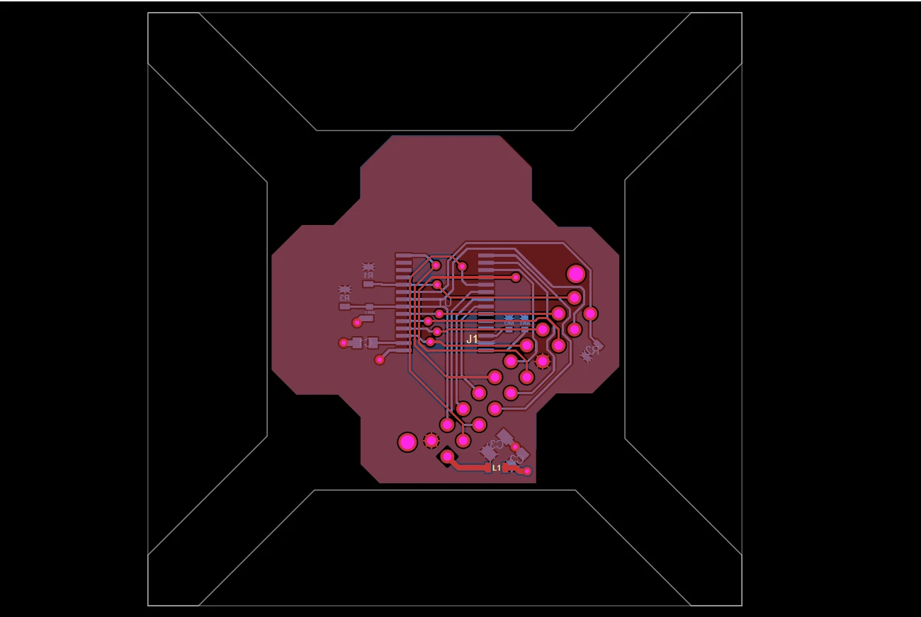
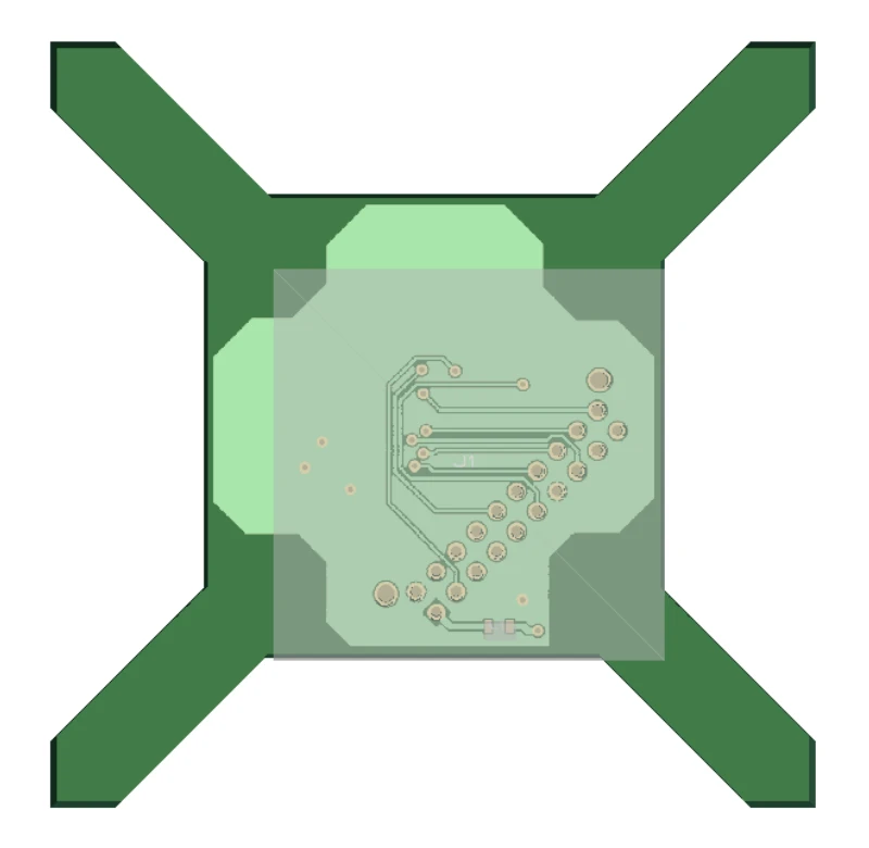
The board on this page is a real, CC0-licensed Allegro 17 export with 12 components, 23 nets and 68 pins. The checks that run on this same board, including the pin match against a tester pin map, are on Board Intelligence.
Measure the copper
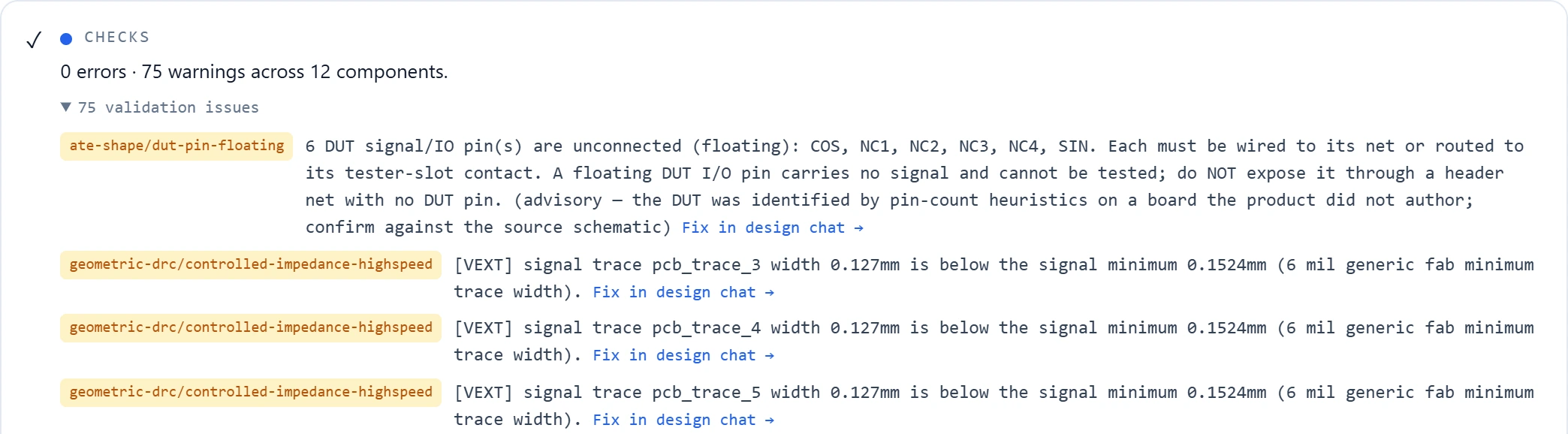
Imported copper is measured, not assumed. Every finding names its rule and gives the measured value next to the threshold, so you can see how far off it is.
Trace width per net class
Supply rails and signal nets, each checked against its own minimum width.
Pad-to-trace clearance
The spacing between copper on different nets, on the same layer.
Annular ring
The copper left around every plated hole and via.
Electrical faults are errors, not warnings: copper of two nets touching on the same layer, a foreign net's trace running through a pad, or a via with no copper contact. A board that is shorted as drawn cannot read as clean. A net with connections but no routed copper is flagged too. As an optional second opinion, where KiCad is installed the board is checked by KiCad's own DRC using ATE·IQ's thresholds, reported separately from ATE·IQ's findings. The full set of board checks is on Board Intelligence.
Follow a requirement onto its copper
The layout binding reconciles the schematic with the routed copper mechanically: same inputs, same answer. That makes the layout more than a picture. Pick a requirement in the layout tab and the traces of its nets are recoloured in the same render, following the chain from requirement to test to net to copper. Tester-side series-termination and Kelvin nets are included when they follow the usual suffix naming (_T, _FORCE, _SENSE). The same chain feeds the traceability dashboard.
Board exports and the fab-readiness gate
Hand the board on in the format the next person needs, from the export menu on the design page. Every export reads the same stored model.
| Export | Contents | Gate |
|---|---|---|
| Gerber + Excellon | Copper layers plus drill files. | fab readiness |
| Fab package | One zip: copper, drills, BOM, pick-and-place, and a readiness README stating what the package contains and what it does not. | fab readiness |
| Pick-and-place | Placement CSV for assembly. | fab readiness |
| BOM | Grouped bill of materials CSV. | — |
| KiCad project | Schematic, board and project files. | — |
| Specctra DSN | Routable netlist; round-trips back through Import SES. | — |
| IPC-2581 Rev C | Connectivity. | — |
| 3D model | The board as a GLB file, from the 3D tab. | — |
| circuit-json | The stored model itself, as a .circuit.json file. | — |
| Schematic PDF | Every sheet, one per page, saved as PDF from the browser. | — |
Fabrication outputs sit behind a readiness gate. A design with no board geometry cannot produce Gerbers that mean anything, so ATE·IQ refuses those exports with the reason stated instead of emitting empty files, and the export menu warns you before you click.