EDA import & export
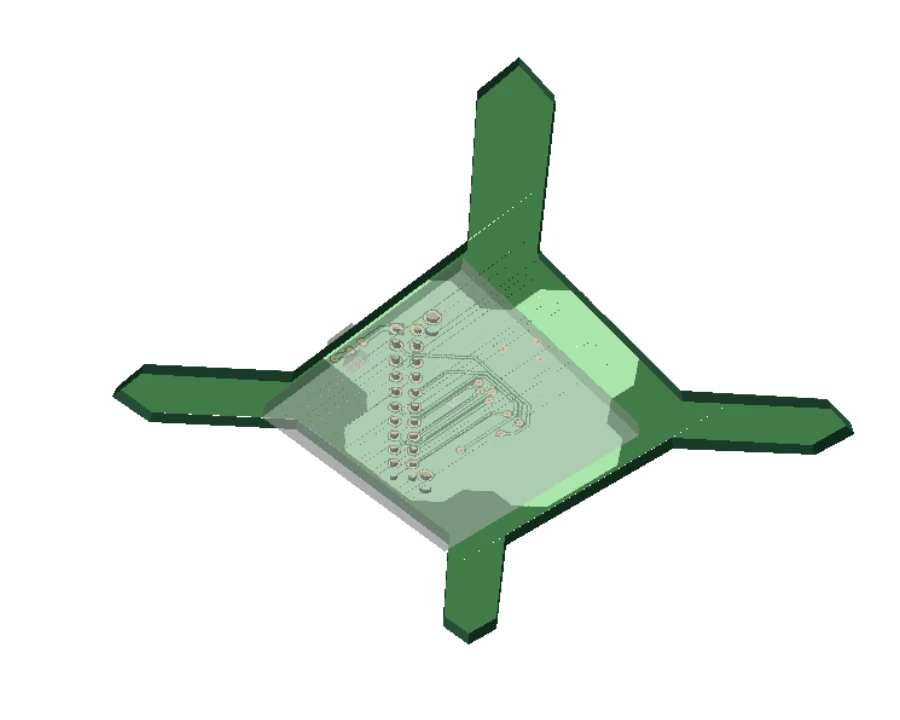
Open the load board your layout tool drew (Cadence Allegro first, then KiCad, EAGLE and the rest), natively, with no Cadence licence needed on your side. View the copper, check the board against the test program’s pins and channel plan, and hand the plan back to the layout engineer as a first draft in the tool’s own inputs. ATE·IQ™ reads, views and verifies boards; the layout stays with the tool that drew it.
- Input
- A Cadence Allegro layout read from its Fabmaster export; a demonstration pin map.
- What ran
- Pin match reconciles the board’s nets against the Pin Map sheet.
- What it found
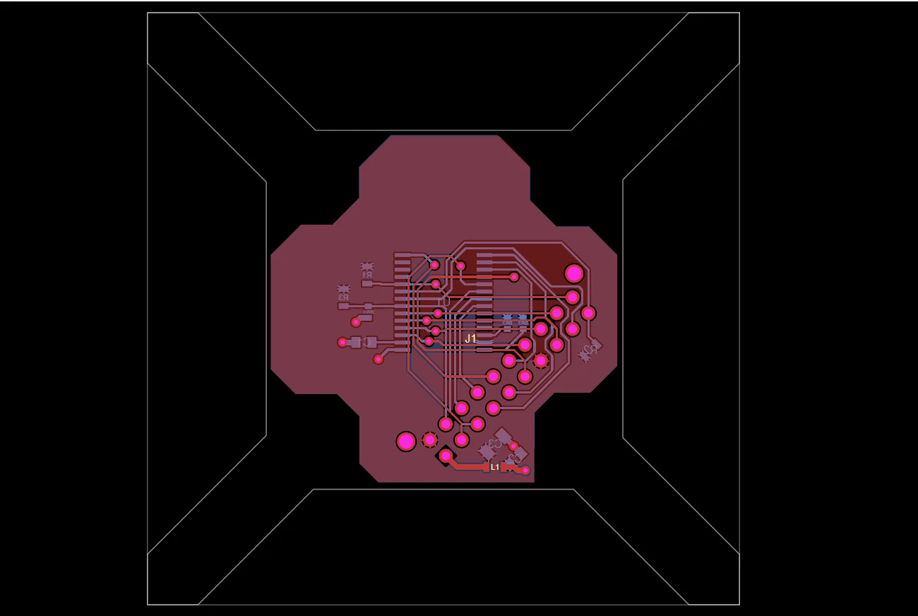
- Pin match on the Cadence Allegro board against a demonstration pin map: 15 of 16 tester pins resolve, and the miss planted in the map on purpose, INDEX, is named as a likely pin-map gap.
Native readers for the exports your layout tool writes
Many DIBs are drawn in Cadence Allegro, and the test engineer rarely has a Cadence Allegro seat. ATE·IQ’s own parsers read what the layout tool exports, so a board arrives with no CAD installation beside ATE·IQ. Pick the files from the Import menu, or link the repository they live in.
| Source | What ATE·IQ builds from it |
|---|---|
| Cadence Allegro Fabmaster (extracta ASCII) | The routed board as Cadence Allegro wrote it (pads, holes, vias, every etch line and arc, the outline, the pours), with real copper in the schematic, layout and 3D views. |
| Cadence Allegro netlist (pstchip · pstxnet · pstxprt) | Components, pins and nets, with a synthesized schematic, enough for the pin match and board↔program sync. |
| IPC-2581 | A layout with real copper, from Cadence Allegro or any tool that writes it. |
| ODB++ (.tgz) | A layout with real copper, rigid-flex boards included. |
| Specctra DSN | The board in its KiCad, Cadence Allegro or EAGLE dialect; round-trips back through an SES session file. |
| KiCad | Native schematics and boards from a synced repository. |
| PDF schematics | A netlist built from the drawing, for boards where the drawing is all you have. |
One command on the layout seat
The layout engineer should not have to guess what to send. ATE·IQ provides an export kit for Cadence Allegro and OrCAD X PCB Editor: one command on the seat writes everything ATE·IQ reads from the board, drives the seat’s own export tools and uploads nothing. The files land beside the board for you to send, and ATE·IQ parses them on your own machine. An export whose artwork films were folded into copper is recognised on import and rebuilt, with a note that says what was set aside and why.
From copper to program and data
Once a board is in, check it against the program that will run on it: pin match reconciles the board’s nets against the Pin Map sheet, the 166-rule DIB check runs over the channel plan and the board, the geometric DRC measures the real copper, and the traceability dashboard carries the chain requirement → test → net → copper → lot. Ask the IG-XL agent about a saved board and it validates and analyses the design in the conversation. Every import carries its provenance and a note that says what the parser read and what it could not; a check whose input is missing says awaiting data and names the step that unlocks it.

And back out
Integration runs in both directions. The program’s channel contract, the saved channel plan, goes back out to Cadence Allegro as the tool’s own inputs: a first-draft netlist and a placement seed, carrying each net’s planned tester channel. The layout engineer starts from the board the program needs, draws the copper in the tool that owns it, and the routed board comes back in through the readers above. An imported board also leaves in the formats other tools take: a BOM, a KiCad project, Specctra DSN, an IPC-2581 netlist (connectivity only) and, where the import carries a schematic, a page to print or save as PDF; Gerbers and the fab package come from the tool that drew it. See PCB layout.